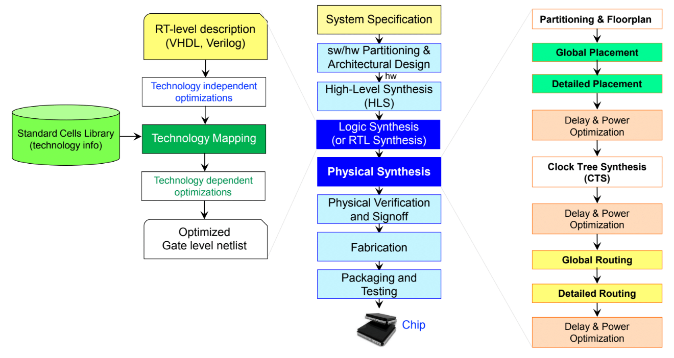

Integrated circuits (ICs) or “chips” are present in practically all electronic devices today. Digital circuit designs, such as processors or video encoders, require a very large number of transistors to be implemented, characterizing VLSI (Very Large Scale Integration) circuits. The design of this type of circuit is based on a design flow (digital flow), which is defined by different steps.
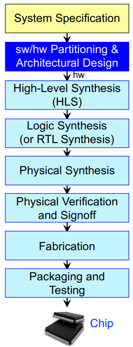
When designing a project, the system to be designed is initially specified: inputs and outputs, functionality, main blocks and others. In the sequence, it is defined which parts of the system will be developed in software and which of them will be developed in hardware. For the hardware part, the application of the VLSI design flow begins.
First, the circuit description is created using hardware description languages (HDL), such as Verilog or VHDL. The functionality of the circuit is checked through an initial simulation without delays and, if no problems are found, the flow continues to the next stage: logical synthesis, in which the circuit description generates a mapping of connections (netlist) using a standard cell library, which includes logic gates, flip-flops, among other components.
The information about standard cells are defined in PDKs (Process Design Kits), which are specific to each of the technologies used, depending on the technological node (channel length of the transistors used, such as 65nm, 45nm, 28nm) and also the foundry (TSMC, Global Foundries and others).
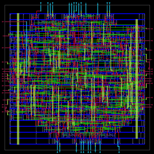
After logical synthesis, physical synthesis takes place, which consists on the process of creating the chip layout, including internal steps such as positioning cells, routing and placing pads (connections to the external world). A new simulation can be performed, now considering more realistic delays of the cells used and the circuit interconnections.
Finally, the circuit must still be verified according to the design rules for the manufacturing technology (DRC) and also the equivalence between the layout obtained and the initial desired schematic (LVS). With the layout complete and validated, it is possible to send the project for manufacturing and subsequently the packaging and testing stages of the new chips.
In addition to the parts of the flow highlighted above, it is worth mentioning that intermediate steps such as Logical Equivalence Check (LEC), extraction of RC parameters, among others, are also part of the flow and are important to ensure the proper functioning of the final product. All synthesis steps are performed automatically by the tool, as well as verifications. As for simulations, normally the designer must develop a testbench to test the architecture, seeking to validate the circuit with the best possible scope and avoiding errors that could lead to the loss of many resources by manufacturing a defective chip.
At ECL, our project flow is done with Synopsys EDA tools. In addition, we have also implemented a completely open source digital design flow for ASICs (application-specific integrated circuits) with tools such as Icarus Verilog, Yosys and OpenROAD. We also work with different technological nodes, in addition to open source and private PDKs from various foundries in the world.