image34

Algorithms and Architectures for Image and Video Processing

Video coding is essential to make the use of digital videos possible. Without it, videos with thirty or sixty frames per second would take up a huge amount of space, making it impossible to store them on mobile devices or even share videos in real time, as it happens in videoconferences. Based on this perspective, encoders act on modifying a sequence of frames in order to reduce the amount of information that must be stored, especially when exploiting the minimization of redundancies between frames. The decoders, in turn, receive the encoded information and must follow the opposite path of the encoder, discovering the necessary information to reconstruct and present the images received.

The standard encoder model is composed of different steps, as illustrated in Figure 1. Inside the encoder, blocks from the original frame will be compared to reference blocks (predicted blocks based on information from past frames or the same frame). The difference between the two blocks (result of the subtraction between the original and the reference) generates what is called a residue, a matrix with much smaller values than the original block and which, therefore, generates a smaller volume of information to be stored.

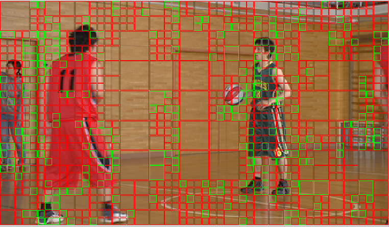
The redundancies present in images can be both spatial (in the same frame) and temporal (between frames). There are, hence, two types of prediction: intra-frames (in the same frame, for spatial redundancy) and inter-frames (between frames, for temporal redundancy). This prediction step determines the reference blocks. The residue then undergoes a transformation, taking its information to the frequency domain, in order to enable filtering of only the most relevant frequency components for human vision. Next, there is the quantification of information and finally the coding of entropy. In this encoding, data that occurs more frequently receives encodings with a smaller number of bits, while less frequent data is mapped to larger sets of bits, in order to reduce the bitstream generated at the end of the encoding process.

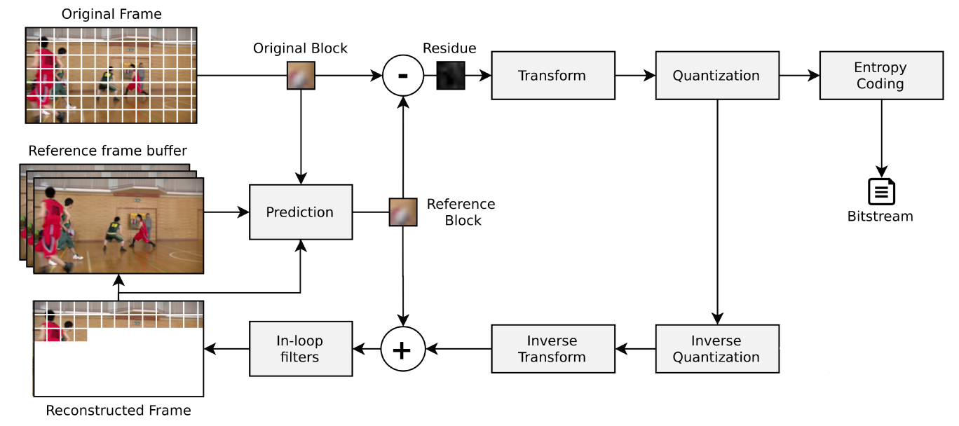
Figure 1: Representation of the video coding steps, adapted from Richardson (2004) [1].

At ECL, we develop hardware solutions for video coding applications, such as architectures for Fractional Motion Estimation (FME), one of the most computationally expensive steps that takes place during inter-frame prediction. Through a dedicated architecture, the aim is to reduce the block’s energy consumption, which is of great importance for video coding, given the need for image and video processing on battery-powered mobile devices.

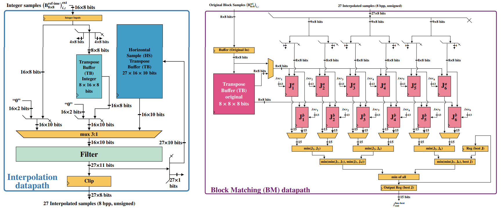
Figure 2: Representation of the interpolation and search modules of the FME architecture developed at ECL.

In addition to the FME, research focused on Approximate Computing (AxC) is also being developed at ECL, which consists of an approach to reduce energy, area and delay in hardware architectures. We evaluate AxC techniques on Gaussian filter architectures to reduce power and area while minimizing loss in resolution quality. Furthermore, we develop research that combines traditional video coding methods with Artificial Intelligence to improve coding efficiency, in addition to studying video post-processing methods, in order to improve the user experience on different platforms.

[1] RICHARDSON, I. E. G. H.264 and MPEG-4 video compression: video coding for next-generation multimedia. West Sussex, England: John Wiley & Sons Ltd, 2004. 206 p.

layout_circuitos_integrados_s

Digital Integrated Circuits Design

Integrated circuits (ICs) or “chips” are present in practically all electronic devices today. Digital circuit designs, such as processors or video encoders, require a very large number of transistors to be implemented, characterizing VLSI (Very Large Scale Integration) circuits. The design of this type of circuit is based on a design flow (digital flow), which is defined by different steps.

VLSI_flow_overview

When designing a project, the system to be designed is initially specified: inputs and outputs, functionality, main blocks and others. In the sequence, it is defined which parts of the system will be developed in software and which of them will be developed in hardware. For the hardware part, the application of the VLSI design flow begins.

First, the circuit description is created using hardware description languages (HDL), such as Verilog or VHDL. The functionality of the circuit is checked through an initial simulation without delays and, if no problems are found, the flow continues to the next stage: logical synthesis, in which the circuit description generates a mapping of connections (netlist) using a standard cell library, which includes logic gates, flip-flops, among other components.

The information about standard cells are defined in PDKs (Process Design Kits), which are specific to each of the technologies used, depending on the technological node (channel length of the transistors used, such as 65nm, 45nm, 28nm) and also the foundry (TSMC, Global Foundries and others).

After logical synthesis, physical synthesis takes place, which consists on the process of creating the chip layout, including internal steps such as positioning cells, routing and placing pads (connections to the external world). A new simulation can be performed, now considering more realistic delays of the cells used and the circuit interconnections.

Finally, the circuit must still be verified according to the design rules for the manufacturing technology (DRC) and also the equivalence between the layout obtained and the initial desired schematic (LVS). With the layout complete and validated, it is possible to send the project for manufacturing and subsequently the packaging and testing stages of the new chips.

In addition to the parts of the flow highlighted above, it is worth mentioning that intermediate steps such as Logical Equivalence Check (LEC), extraction of RC parameters, among others, are also part of the flow and are important to ensure the proper functioning of the final product. All synthesis steps are performed automatically by the tool, as well as verifications. As for simulations, normally the designer must develop a testbench to test the architecture, seeking to validate the circuit with the best possible scope and avoiding errors that could lead to the loss of many resources by manufacturing a defective chip.

At ECL, our project flow is done with Synopsys EDA tools. In addition, we have also implemented a completely open source digital design flow for ASICs (application-specific integrated circuits) with tools such as Icarus Verilog, Yosys and OpenROAD. We also work with different technological nodes, in addition to open source and private PDKs from various foundries in the world.

testes_em_multicore

Multicore Testing

With the exploitation of parallelism and the consequent exponential growth in performance in recent decades, multiprocessor chips (CMP) manufacture is increasing in complexity. CMPs require communication between their cores. Architectures based on messages provide the processor with a local memory that can only be accessed by it, requiring message exchange with the other cores in the system. Architectures based on shared memory make all memory addresses accessible to all cores, enabling communication through loads and stores. The abstraction of a single shared memory requires a conceptual model of memory operations that can be executed simultaneously, so-called Memory Consistency Model (MCM).


In the ever-increasing quest to increase performance, multicore chip manufacturers started to use increasingly relaxed MCMs, where read and write instructions can be executed out-of-the-order specified by the threads of a concurrent program. The growing number of processing cores and the use of relaxed consistency models corroborate the increased complexity of processor designs, making them susceptible to design errors.


Functional verification, in an informal way, is the comparison of what the processor should ideally be and what it currently is. In the context of CMPs, the verification process consists of running concurrent programs on multi-chip simulators and assessing whether the behavior observed corresponds to the expected behavior. Such programs are created automatically by intelligent agents, and the behavior of the MCM of the chip(s) is also automatically evaluated by checkers afterwards (post-morten) or during execution (on-the-fly).


During more than a decade of research, ECL has developed a complex but efficient shared memory functional verification framework. The framework consists of an automatic generator of concurrent programs, a checker, and intelligent agents that direct the automatic creation of tests to reduce verification time and effort by exploiting the characteristics of this problem. Each concurrent program is executed on a multicore, stimulating the shared memory system. The checker automatically verifies whether, when running the program, any observed behavior has disobeyed the multicore’s memory model, which represents a hardware error.


After more than a decade of publications, ECL’s multicore testing group continues to work on automatic test generation to reduce verification time and effort, creating new forms of test representation and intelligent algorithms. In addition to porting the framework for Instruction Set Architectures to SPARC and ARM, RISC-V has emerged as a target for porting and publications.


From this area of research, ECL has produced doctoral theses, master’s dissertations, and scientific initiation projects, publishing high scientific level works and forming qualified professionals, working on AI research in Brazil, as well as in companies in Europe and the United States.


Publications (until 2023):

E. A. Rambo, O. P. Henschel and L. C. V. dos Santos, “Automatic generation of memory consistency tests for chip multiprocessing,” 2011 18th IEEE International Conference on Electronics, Circuits, and Systems, Beirut, Lebanon, 2011, pp. 542-545, doi: 10.1109/ICECS.2011.6122332.

L. S. Freitas, G. A. G. Andrade and L. C. V. dos Santos, “Efficient verification of out-of-order behaviors with relaxed scoreboards,” 2012 IEEE 30th International Conference on Computer Design (ICCD), Montreal, QC, Canada, 2012, pp. 510-511, doi: 10.1109/ICCD.2012.6378698.

E. A. Rambo, O. P. Henschel and L. C. V. dos Santos, “On ESL verification of memory consistency for system-on-chip multiprocessing,” 2012 Design, Automation & Test in Europe Conference & Exhibition (DATE), Dresden, Germany, 2012, pp. 9-14, doi: 10.1109/DATE.2012.6176424.

L. S. Freitas, G. A. G. Andrade and L. C. V. dos Santos, “A template for the construction of efficient checkers with full verification guarantees,” 2012 19th IEEE International Conference on Electronics, Circuits, and Systems (ICECS 2012), Seville, Spain, 2012, pp. 280-283, doi: 10.1109/ICECS.2012.6463746.

L. S. Freitas, E. A. Rambo and L. C. V. dos Santos, “On-the-fly verification of memory consistency with concurrent relaxed scoreboards,” 2013 Design, Automation & Test in Europe Conference & Exhibition (DATE), Grenoble, France, 2013, pp. 631-636, doi: 10.7873/DATE.2013.138.

O. P. Henschel and L. C. V. dos Santos, “Pre-silicon verification of multiprocessor SoCs: The case for on-the-fly coherence/consistency checking,” 2013 IEEE 20th International Conference on Electronics, Circuits, and Systems (ICECS), Abu Dhabi, United Arab Emirates, 2013, pp. 843-846, doi: 10.1109/ICECS.2013.6815546

G. A. G. Andrade, M. Graf and L. C. V. dos Santos, “Chain-based pseudorandom tests for pre-silicon verification of CMP memory systems,” 2016 IEEE 34th International Conference on Computer Design (ICCD), Scottsdale, AZ, USA, 2016, pp. 552-559, doi: 10.1109/ICCD.2016.7753340.

G. A. G. Andrade, M. Graf, N. Pfeifer and L. C. V. dos Santos, “Steep Coverage-Ascent Directed Test Generation for Shared-Memory Verification of Multicore Chips,” 2018 IEEE/ACM International Conference on Computer-Aided Design (ICCAD), San Diego, CA, USA, 2018, pp. 1-8, doi: 10.1145/3240765.3240852.

G. A. G. Andrade, M. Graf and L. C. V. dos Santos, “Chaining and Biasing: Test Generation Techniques for Shared-Memory Verification,” in IEEE Transactions on Computer-Aided Design of Integrated Circuits and Systems, vol. 39, no. 3, pp. 728-741, March 2020, doi: 10.1109/TCAD.2019.2894376.

M. Graf, O. P. Henschel, R. P. Alevato and L. C. V. dos Santos, “Spec&Check: An Approach to the Building of Shared-Memory Runtime Checkers for Multicore Chip Design Verification,” 2019 IEEE/ACM International Conference on Computer-Aided Design (ICCAD), Westminster, CO, USA, 2019, pp. 1-7, doi: 10.1109/ICCAD45719.2019.8942040.

G. A. G. Andrade, M. Graf, N. Pfeifer and L. C. V. dos Santos, “A Directed Test Generator for Shared-Memory Verification of Multicore Chip Designs,” in IEEE Transactions on Computer-Aided Design of Integrated Circuits and Systems, vol. 39, no. 12, pp. 5295-5303, Dec. 2020, doi: 10.1109/TCAD.2020.2974343.

N. Pfeifer, B. V. Zimpel, G. A. G. Andrade and L. C. V. dos Santos, “A Reinforcement Learning Approach to Directed Test Generation for Shared Memory Verification,” 2020 Design, Automation & Test in Europe Conference & Exhibition (DATE), Grenoble, France, 2020, pp. 538-543, doi: 10.23919/DATE48585.2020.9116198.

M. Graf, G. A. G. Andrade and L. C. V. dos Santos, “EveCheck: An Event-Driven, Scalable Algorithm for Coherent Shared Memory Verification,” in IEEE Transactions on Computer-Aided Design of Integrated Circuits and Systems, vol. 42, no. 2, pp. 683-696, Feb. 2023, doi: 10.1109/TCAD.2022.3178051.